Thursday, September 5, 2013

LED Chaser cum Blinker

How to Make a LED Chaser cum Blinker Circuit Using IC 4017


  The presented circuit was requested by Mr.Joe, one of the keen followers of this blog. The circuit initially was intended to be used for generating LED strobe light effects and was asked to be modified such that it could be used as an LED sequencer as well as a blinker. The change over would be implemented via a toggle switch.

The circuit diagram may be understood with the following points:

The IC 4017 is not new to us and we all know how versatile and competent this device is. Basically the IC a Johnson’s decade counter/divide by 10 IC, fundamentally used in applications where sequencing positive output signals are required or desired.

 The sequencing or the orderly shifting of the outputs take place in response to a clock pulse that needs to be applied at the clock input pin #14 of the IC.

With every rising positive edge of the clock input, the IC responds and pushes its output’s positive from the existing pin out to the next pin out in the order.

Here a couple of NOT gates are used as a oscillator for providing the above clock pulses to the IC 4017. VR1 may be adjuted for determining or fixing the speed of the sequencing.

The outputs of the IC are connected to an array of LEDs in a specific order which makes the LEDs look like as if they are running or chasing during the operations.

If the circuit would be required only to produce the chasing effect, the diodes would not be required, however as per the present ask the diodes become important and allows the circuit to be used as a blinker also, depending upon the position of the switch S1.

When the switch S1 is positioned at A, the circuit behaves like a light chaser and produces the normal chasing effect over the LEDs which start illuminating in sequence from top to the bottom, repeating the operations as long as the circuit remains powered.

As soon as S1 is flicked toward B, the clock signals from the oscillator are shifted into the input of the transistor T1, which instantly stats to pulsate all the LEDs together in response to the received clocks from N1/N2 configuration.

Thus as per the requirement we have successfully modified an ordinary light chaser circuit with an additional feature through which the circuit now is also able to function as a LED flasher.

Do not forget to connect the inputs of the remaining unused gates from the IC 4049 either to the positive or the negative of the supply. The supply pins of the IC 4049 also need to be connected to the relevant supply rails of the circuit, kindly refer to the datasheet of the IC.

Tf all the ten outputs of the IC 4017 are required to be integrated with LED sequencing, just connect pin #15 of the IC to ground and use the left over outputs of the IC for the required sequencing of the LEDs in the order of:3,2,4,7,10,1,5,6,9,11

Parts List

The fooliwng parts will be needed for making this LED light chaser cum flaher circuit:

R1, R2, R3 = 1K,
VR1 = 100K linear pot.
All LED resistors are = 470 Ohms,
All diodes are = 1N4148,
All LEDs = RED, 5mm or as per choice,
T1 = 2N2907, or 8550 or 187,
C1 = 10uF/25V
C2 = 0.1uF,
IC1 = 4017,
N1, N2 = IC4049

Simple Infra Red Remote Control

How to make a Simple Infra Red Remote Control Circuit


Controlling household electrical gadgets or any electrical equipment remotely can be fun.  Controlling gadgets like a TV set or a DVD player through a remote may look pretty common to us and we are very used to with the experience, however for controlling many other domestic equipment like a water pump, lights etc we are compelled to walk around for implementing the switching.


The article is inspired by our usual TV remote concept and has been applied for controlling other house hold electrical appliances remotely.  The circuit facilitates and helps the user to do the operations without moving an inch from his resting place.

The whole circuit of the proposed IR remote control may be understood by studying the following points:

Referring to the figure, we see that the entire layout consists of just a couple of stages viz: the IR sensor stage and the fkip flop stage.

Thanks to the highly versatile, miniature IR sensor unit which forms the heart of the circuit and directly coverts the received IR waves from the tranamitter unit into the relevant logic pulses for feeding the fllip flop stage.

The sensor basically consists of just three leads viz: the input, the output and the biasing voltage input lead. The involvmant of only three leads makes the unit very easy to configure into a practical circuit.

The sensor is specified for operating at 5 volts regulated voltage which makes the inclusion of the 7805 IC stage important. The 5 voltage supply also becomes useful for the flip flop IC 4017 and is appropriately supplied to the relevant stage.

When a IR signal becomes incident over the sensor lens, the inbuilt feature of the unit activates, triggering a sudden drop in its output voltage.

The PNP transistor T1 responds to the negative trigger pulse from the sensor and quickly pulls the positive potential at its emitter to the collector across the resistor R2.

The potential developed across R2 provides a positive logic high to the IC 4017 input pin #14. The IC instantly flips its output and changes it’s polarity. 

The transistor T2 accepts the command and switches the relay according to the relevant input provided to its base.

The relay thus switches the connected load across its contacts alternately in response to the subsequent triggers received from the IR transmitter unit.

For the sake of convenience the user may use the existing TV remote control set unit as the transmitter for operating the above explained control circuit.

The referred sensor is well compatible with all normal TV or DVD remote control handset and thus can be appropriately switched through it.

The entire circuit is powered from an ordinary transformer/bridge network and the entire circuit may be housed inside a small plastic box with the relevant wires coming out of the box for the desired connections. 
Parts List  

The following parts will be required for making the above explained infra red remote control circuit:

R1, R3 = 100 ohms,
R2 = 100K,
R4 = 4K7,
R5 = 10K,
C2 = 470uF/25V
C1, C4= 22uF/25V,
C6 = 4.7uF/25V,
C3 = 0.1, CERAMIC,
C5 = 1000uF/25V,
T1 = BC557B
T2 = BC547B,
ALL DIODES ARE = 1N4007,
IR SENSOR = TSOP1738 image: Vishay
 IC1 = 4017,
IC2 = 7805,
TRANSFORMER = 0-12V/500mA,

Automatic 12 volt Battery Charger

How to Make an Automatic 12 volt Battery Charger Circuit Using IC LM 338


The IC LM338 is an outstanding device which can be used for unlimited number of potential electronic circuit applications. Basically the main function of this IC is voltage control and can also be wired for controlling currents through some simple modifications. Battery charger circuit applications are ideally suited with this IC and we are going to study one example circuits for making a 12 volt automatic battery charger circuit using the IC LM338.

Referring to the circuit diagram we see that the entire circuit is wired around the IC LM301, which forms the control circuit for executing the trip off actions. 

The IC LM338 is configured as the current controller and as the circuit breaker module. The whole operation can be analyzed trough the following points:

The IC LM 301 is wired as a comparator with its non inverting input clamped to a fixed reference point derived from a potential divider network made from R2 and R3.

The potential acquired from the junction of R3 and R4 is used for setting the output voltage of the IC LM338 to a level that’s a shade higher than the required charging voltage, to about 14 volts.

This voltage is fed to the battery under charger via the resistor R6 which is included here in the form of a current sensor.


The 500 Ohm resistor connected across the input and the output pins of the IC LM338 makes sure that even after the circuit is automatically switched OFF, the battery is trickle charged as long as it remains connected to the circuit output.

The start button is used to initiate the charging process after a partially discharged battery is connected to the output of the circuit.

R6 may be selected appropriately for acquiring different charging rates depending upon the battery AH.


Circuit Functioning Details (As Explained By +ElectronLover)

" As soon as the connected battery is charged fully, the potential at the inverting input of the opamp becomes higher than the set voltage at non-inverting input of the IC. This instantly switches the output of the opamp to logic low."

According to me:
V+ = VCC - 74mV
V- = VCC - Icharging x R6
VCC= Voltage on pin 7 of Opamp.
When The battery charges fully Icharging reduces. V- become greater than V+, output of the Opamp goes low, Turning on the PNP and LED.
Also,
R4 gets a ground connection through the diode. R4 becomes parallel to R1 reducing the effective resistance seen from the pin ADJ of LM338 to GND. 
Vout(LM338) = 1.2+1.2xReff/(R2+R3), Reff is the Resistance of pin ADJ to GND.

When the Reff reduces the output of LM338 reduces and inhibit charging.


Metal Detector

How to Make a Simple Metal Detector Circuit Using IC CS209A


The principle of operation of the proposed metal detector circuit is quite basic yet very interesting. The detecting function is triggered by sensing the decrease in the Q level of the LC network associated with the circuit in the presence of a metal at a specified proximity level.

Basically the built-in oscillator of the IC CS209 is made functional with the inclusion of a parallel resonant LC tuned network in conjunction with a feedback resistor wired up with the OSC and RF pin outs.

The impedance of the tuned resonant network may be expected at the maximum level as long as the driving source frequency is equal to the resonant frequency of the LC circuit network.

On detecting the presence of a metallic object at a close proximity to the inductor sensor, the voltage amplitude of the LC network gradually begins to fall corresponding to the closeness of the metal to the inductor.

Due to the above factor when the oscillation frame of the chip drops and reaches a certain threshold level, triggers the position of the complementary outputs such that they change states.


More technically the operation may be understood as follows:

Referring to the figure, as soon as a metal object is detected at the inductor input, the capacitor connected to the DEMOD gets charged through an in built current source of 30 uA.

However during the detection process the above current gets deviated away from the capacitor proportionately with the generated negative bias on the LC network.

Therefore the charge from the capacitor is removed attached to DEMOD with every negative cycle generated across the LC network.

The DC voltage with ripple over the capacitor of the DEMOD is then directly referenced with an internal fixed 1.44 voltage level.

When the procedure forces the internal comparator to trip, it switches the transistor which introduces a 23.6 K Ohms in parallel to the given 4K8 resistor.

This resulting reference level then equals near about 1.2 volts which introduces some sort hysteresis in the circuit, and becomes ideally suited for preventing wrong or false triggering.

The feedback pot connected across the OSC and the RF is used for setting the detection range of the circuit.

Increasing the resistance of the pot, in course increases the range of detection and subsequently the tripping point of the outputs.

However the detection and the trip points may also be dependant on the LC configuration and the Q of the LC network.

How to Set up the Metal Detector Circuit

The proposed metal detector circuit may be set up initially by following the below described steps:

Position a metal object at relatively larger distance away from the inductor, assuming the Q of the LC to be at the maximum sensitivity and the distance to be within the allowable range provided by the Q factor of the inductor.

With this set up adjust the pot such that the outputs just shift states indicating the detection of the metal object.

Repeat the adjustment procedure by gradually increasing the distance until a suitable maximum sensitivity of the circuit is optimized.

Removing or displacing the metal manually should make the output of the circuit to revert states, confirming the perfect working of the circuit.

Though the circuit is able to detect metals within a range of 0.3 inches, the range may be suitably increased by increasing the Q of the inductor.

The Q factor is directly proportional with the sensitivity of the circuit and the degree of detections.

Light Activated Day Night Switch

How to Make a Light Activated Day Night Switch Circuit – Science Fair Project


 The circuits explained here can all be used for controlling a load, normally a lamp, in response to the varying levels of the surrounding ambient light. The circuit can be used as a commercial automatic street light control system, as a domestic porch light or corridor light controller or simply can be used by any school kid for displaying the feature in his school fair exhibition. 


The following content describes four simple ways of making a light activated switch using different methods. 

The first diagram shows how the circuit can be configured using transistors, the second and the third circuits demonstare the principle by using CMOS ICs while the last circuit explaines the same concept being implemented using the ubiquitous IC 555.

Let’s evaluate the circuits one by one with the following points:

The first figure shows the use of a couple of transistors in association with a few other components lke resistors for the construction of proposed design.
 The transistors are rigged as inverters, meaning when T1 switches, T2 is switched OFF and vice versa.
The transistors T1 is wired as a comparator and consists of an LDR across its base and the positive supply via a preset.

The LDR is used for sensing the ambient light conditions and is used for triggering T1 when the light level crosses a particular set threshold. This threshold is set by the preset P1.

The use of two transistors particularly helps to reduce the hysteresis of the circuit which would have otherwise affected the circuit if only a single transistor would have been incorporated.

When T1 conducts, T2 is switched OFF ans so is the relay and the connected load or the light.
The opposite happens when the light over the LDR falls or when darkness sets in.

The second and the third figure incorporates CMOS ICs for executing the above functions and the concept remains rather similar. The first circuit out of the two utilizes the IC 4093 which is quad two-input NAND gate IC.


Each of the gates are formed into inverters by shorting its both the inputs together, so that the input logic level of the gates now get effectively reversed at thie outputs.

Though a single NAND gate would be enough for implementing the actions, three gates have been engaged as buffers for getting better results and in a view of utilizing all of them as in any case three of them would be left idle.

The gate which is responsible for the sensing can be seen accompanied with the light sensing device LDR wired across its input and the positive via a variable resistor. 

This variable resistor is used for setting the triggering point of the gate when the light falling over the LDR reaches the desired specified intensity.

As this happens, the gate input goes high, the output consequently becomes low making the outputs of the buffer gates high. The result is the triggering of the transistor and the relay assembly. The connected load over the relay now flips into the intended actions.


The above actions are exactly replicated using the IC 4049 which is also wired with similar configuration and is quite explanatory.

The last figure illustrates how the IC 555 may be configured for executing the above responses.


Parts List

R1 = 1M
R3 = 2m2
C1 = 0.1uF
Rl1 = 12V, SPDT,
D1 = 1N4007,
N1----N6 = IC 4049
N1----N4 = IC 4093
IC1 = 555

Over Head Tank Water Level Indicator cum Controller Circuit

How to Make Over Head Tank Water Level Indicator cum Controller Circuit


The circuit provided in this article performs a dual function of both, as an over head tank water level indicator as well as a controller. The indications of the rising water are provided by five LEDs, which light up sequentially in response to the rising water level inside the tank.


As soon as the water reaches the uppermost level of the tank, the last sensor positioned at the relevant point triggers a relay which in turn switches the pump motor for initiating the required water evacuating action.

The circuit is as simple as it could be. Use of just one IC makes the entire configuration very easy to build, install and maintain.

The fact that impure water which happens to be the tap water that we receive in our homes offers a relatively low resistance to electricity has been effectively exploited for implementing the intended purpose.

Here a single CMOS IC 4049 has been employed for the necessary sensing and executing the control function.

Another interesting associated fact that’s associated with CMOS ICs has helped in making the present concept very easy to implement.

It is the high input resistance and sensitivity of the CMOS gates which actually makes the functioning completely straightforward and hassle free.

As shown in the figure, we see that the six NOT gates inside the IC 4049 are arranged in line with their inputs directly introduced inside the tank for the required sensing of the water levels.

The ground or the negative terminal of the power supply is introduced right at the bottom of the tank, so that it becomes the first terminal to come in contact with water inside the tank.

It also means that the preceding sensors placed inside the tank, or rather the inputs of the NOT gates sequentially come in contact or bridges themselves with the negative potential as the water gradually rises inside the tank.

We know that NOT gates are simple potential or logic inverters, meaning their output produces exactly the opposite potential to the one that’s applied to their input.

Here it means as the negative potential from the water bottom comes in contact with the inputs of the NOT gates through the resistance offered by the water, the output of those relevant NOT gates sequentially start producing opposite response, that is their outputs start becoming logic high or become at the positive potential.

This action immediately lights up the LEDs at the outputs of the relevant gates, indicating the proportionate levels of the water inside the tank.

Another point that’s to be noted is, all the inputs of the gates are clamped to the positive supply through a high value resistance.

This is important so that the gates inputs are initially fixed at the high logic level and subsequently their outputs generate a logic low level keeping all the LEDs switched off when there’s no water present inside the tank.

The last gate which is responsible for initiating the motor pump has its input positioned right at the brim of the tank.

It means when the water reaches t the top of the tank and bridges the negative supply to this input, the gate output becomes positive and riggers the transistor T1, which in turn switches the power to the motor pump through the wired relay contacts.

The motor pump stats and begin evacuating or releasing the water from the tank to some other destination.

This helps the water tank from overfilling and spilling, the other relevant LEDs which monitors the level of the water as it climbs also provides important indication and information regarding the instantaneous levels of the rising water inside the tank.

Parts List

R1 to R6 = 2M2,

R7 to R12 = 1K,

All LEDs = Red 5mm,

D1 = 1N4148,

Relay = 12 V, SPDT,

T1 = BC547B

N1 to N5 = IC 4049

All the sensor points are ordinary brass screw terminals fitted over a plastic stick at the required measured distance apart and connected to the circuit through flexible conducting insulated wires (14/36)

Versatile Timer Circuit

How to Make a Simple Versatile Timer Circuit Using IC 4060


I have already discussed this IC comprehensively in one of my previous articles, everything regarding its pin outs have discussed there in detail. We studied there that the IC 4060 is specifically suited for timer applications and also as an oscillator. In this article we’ll study how a simple versatile timer can be built using the IC 4060.


Other than the IC you would require just a couple of resistors, one pot and a capacitor for making this timer.
Referring the figure, the simplicity of the design becomes evident and therefore this circuit is perfectly suited for all electronic newcomers, who can easily buildthis project and enjoy its useful service.

As explained earlier in one my articles, the IC has an in built oscillator that needs just a few passive external components for making it tick.

Depending upon the values of the external RC components, the oscillation periods can be varied right from a few fractions of a second to many hours.

RC components refer to the values of the external time determining components consisting of a resistor or a pot and a capacitor.

The outputs produce a varied rate of time periods; each output generates time periods that’s exactly double to that of the previous output in a certain order of the IC pin outs.

Since here we want to use this unit as a timer we have selected the pin out which is last in the order as far the length of the time period is concerned, meaning we have selected pin #3 which generates the highest delay period.

The biggest advantage of making a timer using IC 4060 is that the involved timing capacitor cam ne kept as small as possible by increasing the complementary timing component value, which is the resistor. 

This helps to keep the circuit simple, smaller and very sleek, unlike other timer IC like 555 which require high value electrolytic capacitors for generating even ordinary time delays.

In the figure you can see a diode being introduced from the output pin #3 to one of the oscillator pin #11. This diode acts as a latching component, which latches the IC once the set time lapses and the output of the IC goes high.

If this diode is not inserted, the output would go freewheeling from logic high to logic low and keep repeating the time delays.

The circuit may be powered from a small 9 volt battery which will last almost for ever.

A buzzer is fitted at the output for the required indications of the timer output after the time delay has elapsed.

The IC may be reset simply by pressing the reset button or alternatively the circuit gets automatically reset when switched off and powered again.


How to Calculate Frequency or Time Delay of IC 4060 - The Formula


Timer Circuit

How to Make a Simple Timer Circuit Using IC 555


A timer is a device which produces a delay period after which an external connected electrical load is triggered. The produced time delay is normally adjustable and the user has the freedom to set the time period as desired. There are many ways of making simple timer circuits using different ICs and discrete components; here we discuss one such circuit using the ubiquitous IC 555.


The IC 555 is a pretty common electronic part among the electronic enthusiasts and is also very popular due to the involved simple configurations and low component count.

The two popular multivibrator modes of operation that’s associated with this IC are the astable mode, and the monostable mode. Both of these are useful configurations and have plenty of different applications.

For the present design we incorporate the second mode of operation, which is the monostable mode.

In this mode of operation the IC is configured to receive a trigger externally, so that it’s output changes state, meaning if with reference to the ground if the output of the IC is zero, then it would become positive as soon as the trigger (momentary) is received at its input terminal.

This change in its output is sustained for a certain period if time, depending upon the external time determining components. Normally the time determining components are in the form of a resistor and a capacitor which together determine or fix the time period for which the IC output would hold its “high” position.

By changing either the value of the capacitor or the resistor, the timing can be altered as desired. The above time fixing components are termed as the RC component.

The figure shows a very straightforward design where the IC 555 forms the central controlling part of the circuit. As discussed in the above section, the IC is in its standard monostable mode.

Pin #2 receives the external timing trigger from a push-to-ON switch. Once this switch is pushed, the circuit pulls its output to a positive potential   and holds it until the predetermined time delay lapses.

The entire circuit can be built over a small piece of general PCB and housed inside a neat looking plastic enclosure along with the battery.

The output may be ideally connected to a buzzer for receiving the warning alarm after the set time lapses.

Parts List

R1, R4 = 4K7,
R2 = 10K,
R3 = 1M pot,
C1 = 0.47uF,
C2 = 1000uF/25V,
C3 = 0.01uF,
IC1 = 555,
Bz1 = Piezo Buzzer,
Push Button = push to ON switch

A circuit design requested by Mr.Bourgeoisie:


Wireless Speaker System

How to Make Wireless Speaker System - Make Your Own Radio Station Science Project


The article explains a very simple circuit of a wireless speaker system which can be used for playing hi quality music wirelessly from your TV set, DVD player, Ipod, cell phone or from any music system. The speaker thus can be placed in any corner of the house within a radial distance of 50 meters and high quality music can be enjoyed without the hassles of long connecting wires.


For implementing the entire wireless speaker system, we actually need to make two sets of circuits, a transmitter circuit for transmitting the music signal from the source input as discussed above and a receiver circuit for receiving the transmitted music signal and for playing it in the attached speaker.

Transmitter Circuit:

As shown in the figure, the configuration looks a little different from the usual single transistor transmitter circuits where a single stage is used for the audio amplification and for the generation of the modulated carrier waves.

The usual single transistor transmitter circuit has the advantage of smaller and compact size and minimal power consumption, but is not suitable for long and strong signal transmissions. 

However since such circuits are commonly used for wireless, stage-microphone applications, the distance is not a factor but compactness and low power consumption  is definitely a must, and therefore becomes quite suitable for the intended application.

The present design is not intended for the above application so the first two features are not important, however the proposed idea of a wireless speaker system surely requires a long range and a distortion free power transmission, so that the reception can be heard at any corner of a particular premise or even across an apartment.

Therefore a stronger signaling or transmission of stronger carries RF signals becomes a necessity.

That’s exactly why we have incorporated a couple of extra stages in addition to the central carrier wave generator stage.

The first transistor and its associated components form a neat little audio amplifier stage and also a buffer between the audio source and the transmitter circuit.

This stage amplifies the received signal to stronger levels, and this stage also allows keeping the volume of the source signal to minimum levels.

The amplified signal is passed on to the next stage, which is the actual RF signal generator stage.

This stage is basically a simple feedback type of oscillator, wired to produce RF signals in the range of around 90 to 100 Mhz.

The amplified signal from the collector T1 start forces T2 to modulate the generated RF with the injected audio signals.

The modulated signal from the collector of T2 can also be directly used for the intended wireless music receiving, however since we are interested in making it more powerful, we introduce another stage which becomes responsible for amplifying the modulated signals to much stronger levels so that it may be heard across many 10s of meters away and even in cell phone radios.

The inductor L1 is the most critical part of the circuit. Its dimensions are: 1mm, super enameled copper wire, having 5 turns of 6mm diameter. The tap to C6 is taken by scratching the second last turn of the coil toward the positive side end.

The whole transmitter circuit can be built over a small piece of veroboard and housed inside a suitable sized metal box along with the required power supply section enclosed.
This concludes the transmitter circuit.

The Receiver Circuit

Ideally you won’t need to build this as the receptions can be heard crystal clear over an ordinary FM radio set. Therefore you might just want to use the FM radio itself as the wireless loudspeaker, or probably add an ampli-speaker box in conjunction to you FM receiver.
That’s it, your wireless speaker box system is ready and may be used for listening to any audio transmission without connecting wires across a radial distance of more than 50 meters, if the antenna is made large enough, the range may be well increased to beyond 90 meters.

Parts List

R1 =1M,
R2 = 2K2,
R3 = 470 Ohms,
R4 = 39K,
R5 = 470 Ohms,
C1 = 0.1 uF,
C2 = 4.7 uF,
C3, C6 = 0.001uF,
C4 = 3.3pF,
C5 = 10pF,
C7 = 100uF/16V
D1----D4 = 1N4007
L1 = See Text
T1, T2 = BC547B,
T3 = BC557B
TR1 = transformer, 0-9V, 100mA

Rain Sensor

How to Build a Simple Rain Sensor Circuit Using IC 555 - Science Fair Project


This is a simple science project which can be built by a school grade student very easily and can be used for displaying its relatively useful feature, probably among his friends or in a science fair exhibition. The circuit is basically rigged as a comparator and is typically configured to sense the low resistance through water across its relevant inputs.

Let’s try to understand how to build a simple rain sensor circuit using the IC 555:


Referring the figure, we see a rather simple design made around a single active component which is the IC 555.

Other than the IC, the circuit just includes a few cheap passive components likeresistors and capacitors.

We are familiar the two important modes of operation of the IC 555, which are the astable and the monostable multivibrator mode, howver the IC is laid down in a rather unusual fashion, quite like a comparator.

As shown in the figure, sensing terminals are received across the positive and pin #2 of the IC via R1.

When water (due to rain fall) comes across the above inputs, a low resistance is developed here. The preset P1 is suitably adjusted such that any type of water across the sensing inputs triggers the IC appropriately.

 The sudden low resistance at pin #2 of the IC acts like a pulse which exceeds the potential at pin #2 more than 1/3 of the supply voltage.

This activation instantly makes the output of the IC go low, ringing the connected buzzer. The buzzer circuit is comprehensively explained here, if you wanted to build one.

As long as the sensing input stays immersed under water, the output continues with the above situation.

However the moment, water is removed from the specified input terminals, the potential at pin #2 reverts to less than 1/3 of the supply voltage, making the output go high, back to its original position, switching off the buzzer.

The above operation effectively indicates the commencement of a rain fall when the sensor is appropriately placed for the detection.

The charge inside the capacitor C1 keeps the buzzer ringing for some period of time even after the water from the sensing inputs is completely removed.

 Therefore the value of C1 must be appropriately chosen, or may be completely eliminated if the feature is not required.


Making the Sensor Unit.

The circuit obviously needs to be placed indoors, therefore only the sensor terminals are required to be positioned outdoors through long connecting flexible wires.
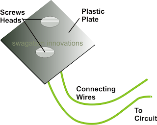
The figure shows a simple way of making the sensor unit.
A small plastic of around 2 by 2 inches is used and a couple metal screws are fixed over the plate. The distance between the screw should be such that no residual water is able to stick or clog between them and water formation across it is detected only as long as the rain fall persists.
The wires from the screws should be carefully terminated to the relevant points on the circuit. The circuit must be hosed inside a suitable plastic enclosure along with the buzzer and the battery.

Parts List

R1 = 1M,
R2 = 100K,
P1 = 1M preset, can be replaced with a 1M fixed resistor
IC = 555,
C1 = 10uF/25V, optional

Rain Sensor/Alarm Circuit Using the IC LM324


Earth Leakage Circuit Breaker

How to Make a Homemade Earth Leakage Circuit Breaker (ELCB) Unit Using IC 324


An earth leakage circuit breaker is a safety electrical device used for monitoring current leakages through the “earthing” terminal and switching OFF the mains when this leakage exceeds a certain dangerous level.
Normally electromechanical concepts are employed for making these devices, however here we will see how an ELCB can be made by using ordinary electronic components; we will also see why an electronic counterpart is more efficient than the commercial electromechanical units.


There are three versions through an electronic ELCB can be made, the first uses a relay for the switching actions, the second idea incorporate a Triac and the third concept employs a SSR or a solid state relay for the required implementations.
For all the above concepts, the triggering feature remains the same, through an input inductor stage.

ELCB Circuit Using Relay

Looking at the figure we can see that the entire circuit is concentrated around a single Opamp from the IC 324. The op amp is configured as a high gain inverting amplifier.
The op amp is configured as a high gain AC amplifier and its sensitivity can be adjusted by varying the value of R2, increasing its value increase the sensitivity of the circuit.
Any minute AC signal that may be present at the inverting input #2 of the IC is picked via the coupling capacitor C1 and instantly amplified by the IC.
A small inductor transformer is wired across the above input of the IC. The primary of the inductor is connected to the wire which finally terminates to the earthing terminal or the pin of the various 3-pin sockets in the premise.
The transformer can be an ordinary output transformer used in small radio receiver’s output amplifier stage.
In case of a leakage, the leaking current passes through the primary winding of the inductor and gets stepped up at the secondary winding.
The stepped up induced AC is immediately sensed by the IC input and further amplified to the desired levels, so that the SCR switches in response to the triggering.
The SCR, due to its inherent property instantly latches and pulls the relay into conduction.
The relay conducts and switches OFF the mains power to the three pin sockets, switching of the appliances and thus eliminating earth leakage conditions

ELCB Circuit Using  a Triac

The above circuit can also be implemented using a Triac, everything remains the same, except the relay stage, which now gets replaced by a Triac.
During normal conditions the IC output remains switched OFF and the triac is allowed to conduct and operate the load.
However the moment a leakage is sensed, the IC output goes high, which triggers the SCR and latches its anode to ground. This inhibits the gate current to the triac which instantly stops conducting, switching OFF the load and rectifying the unfavorable conditions.


ELCB Circuit Using an SSR or SolidState Relay

Mians operated SSR devices are nowadays being effectively employed for switching mains operated loads more efficiently than relays and since these are electrically isolated and solid state in nature, becomes more desirable than the conventional switching devices like triacs and relays.
Here, as long as the conditions are normal, the SSR is able to derive the required input triggering voltage from the circuit, however the moment a leakage is anticipated, the circuit triggers the SCR which in turn chokes the SSR input trigger to ground. The SSR instantly stops conducting, implementing the intended actions by tripping the load and prevents any possible hazard.


Parts List

R1 = 100K,
R2 = 1M,
R3, R4, R5 = 1K,
C1 = 0.01uF
C2 = 100uF/25V
L1 = ordinary small output transformer as used in transistor radios.
SCR = BT169
Triac = BT 136 or higher current type
Op amp = ¼ IC324
SSR = As per user specs.
Relay = 12V, SPDT